Most trainer kits available in the market start showing wrong results after a few years of usage due to the aging of components. This ADC-DAC Trainer tool would work accurately for many more years.
Analog-to-digital converters (ADC) and digital-to-analog converters (DAC) are integral parts of data processing and widely used industrial and household electronic devices. Different conversion methods include resistor ladder, binary weightage, and cascaded op-amp.
The project uses Arduino IDE as the software development platform, so the trainees can perform ADC and DAC experiments as well as get an idea about the configurations of ADC and DAC in Arduino. The main advantages of Arduino software are easy editing and debugging.
ADC-DAC Trainer Circuit Diagram
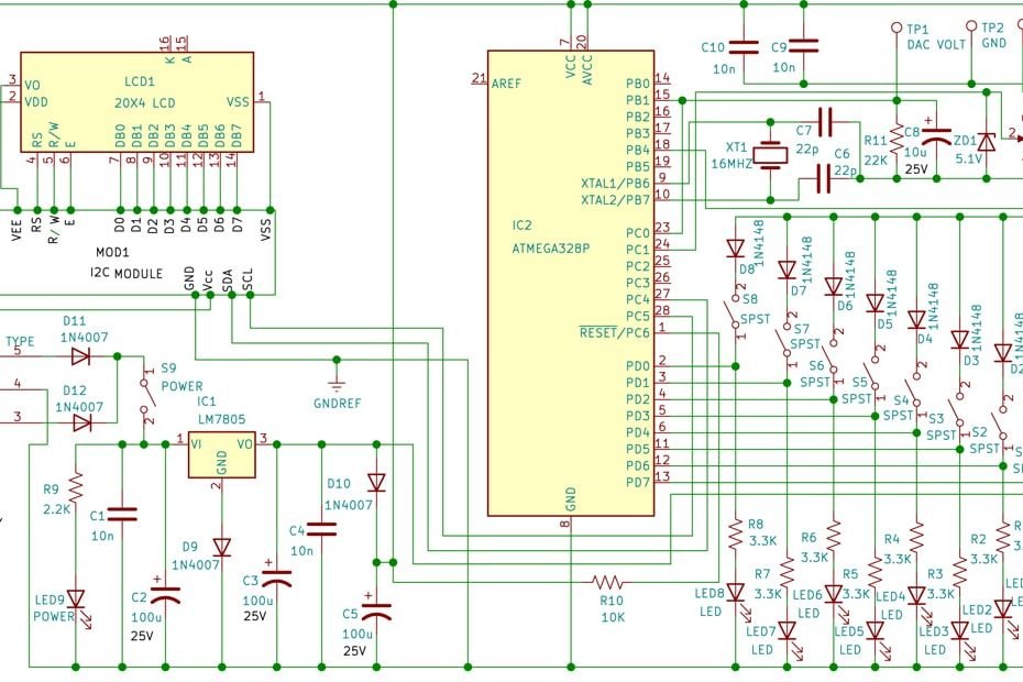
Fig. 1 shows the circuit diagram of the DAC-ADC trainer. The circuit consists of an ATmega328P microcontroller interfaced with a 20×4 LCD module and I2C module, 8-bit LED digital word display/generator, voltage regulator, voltage divider circuit for ADC input, and nine switching diodes, besides some discrete components such as resistors and capacitors.
The ATmega328P microcontroller used in Arduino Uno has six inbuilt ADCs with 10-bit resolution and six DACs with an 8-bit resolution that uses pulse width modulation (PWM) for DAC conversion. The Arduino IDE is known to be the most popular and cost-effective software development platform.
This circuit using the ATmega328P microcontroller can be seen at www.arduino.cc. The ADC input can be from any of the six inbuilt ADCs in the chip.
In the circuit, the 9V-0-9V AC output of 230V AC step-down transformer X1 is rectified by diodes D11 and D12 and smoothened by capacitors C1 and C2. This 9V DC is connected to the input of regulator IC 7805, which converts it into 5.6V through diode D9. Diode D10 converts it to 5V, which is used as a positive supply to the circuit. Filter capacitors C3, C4, and C5 smoothen the supply voltage.
During operation, the power supply may fall slightly below 5V. The ADC input is connected from a 5.6V supply rail to calibrate the maximum ADC input to exactly 5V using pot VR2. Zener diode ZD1 is connected as protection for the ADC pin.
The circuit mainly works in two modes, ADC and DAC. When switch S10 is on, the device operates in DAC mode. When the switch is off, it toggles to ADC mode.
Diodes D1-D8 are used to show exact data generated by the microcontroller in ADC mode. Improper selection of switch S1-S8 in this mode may cause to light up improper LEDs. The protection diodes D1-D8 prevent the supply from the microcontroller to the common supply rail of DAC input and ensure proper LEDs light up.
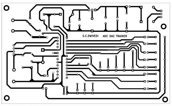
ADC-DAC Trainer PCB
The I2C module and 20×4 LCD are used for hardware simplicity. The controller SCL and SDA pins (A4 and A5 of I2C) are connected to the PC5 and PC4 pins of IC2. The ATmega328P runs at an oscillator frequency of 16MHz because crystal XT1 and capacitors C6 and C7 act as decoupling capacitors.
Resistors R1-R9 are current-limiting resistors for respective LEDs. LED9 is for power-on indication and switch S9 is the power-on/off switch. Resistor R11 and capacitor C8 convert the PWM DAC output to normal DC voltage. As per the datasheet of ATmega328P, capacitors C9, and C10 should be connected as near as possible to the power pins of the controller chip during assembly.
The software is written in Arduino C language Sketch and is well explained in the code. The software uses a special technique of employing a single port for input and output, which may be called port manipulation. Special libraries used in the software are Liquid so goodI2C.h and wire.h. Their installation process is available at online sites.
Construction and Testing
Download Arduino IDE from www.arduino.cc and complete the installation process. Open Arduino IDE and install the libraries. Download the source code file and compile Sketch using Arduino IDE. Connect Arduino Uno to your computer and select the proper port and board. Upload Sketch (ADCDAC_Sketch.ino). For further information, visit www.arduino.cc
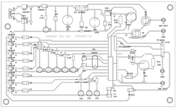
Assemble all the components on a general-purpose PCB with a proper soldering iron. An actual-size, single-side PCB layout for the trainer circuit is shown in Fig. 2 and its component layout in Fig. 3. Make all the wiring as per the circuit diagram (see Fig. 1). Cross-check for any wrong connections. Remove the programmed ATmega 328P IC from Arduino and insert it in its socket (ensure proper orientation).
(Note. I2C module and 20×4 LCD need to be connected externally using jumper wire as their footprints are not given in the PCB layout.)
When you switch on the 230V power supply through switch S9, the LCD will show the welcome messages written in the software. The LCD will thereafter display all the further procedures.
To calibrate, switch on the unit and ensure switch S9 is in ADC mode, that is, it is connected to the 5V power supply. Connect a multimeter across test points TP3 and TP4 and select the 20V DC range.
| Components Required: | |
| IC1 | – 7805, 5V voltage regulator |
| IC2 | – ATmega328P (with Arduino Boot loader) |
| D1-D8 | -1N4148 signal diode |
| D9-D12 | -1N4007 rectifier diode |
| ZD1 | -1N4733 diode |
| LED1-LED9 | – 5mm LED |
| Resistors (all 1/4-watt, ±5% carbon): | |
| R1 | -10-kilo-ohm |
| R2-R12 | -1-kilo-ohm |
| R1-R9 | -5.6-kilo-ohm |
| R1 | -10-kilo-ohm |
| R11 | -22-kilo-ohm |
| VR1 | -10-kilo-ohm 10-turn pot |
| VR2 | -2-kilo-ohm pot |
| Capacitors: | |
| C1, C4, C9, C10 | -10nF ceramic disc |
| C2, C3, C5 | -100uF, 25V electrolytic |
| C6, C7 | -22pF ceramic disc |
| C8 | -10µF, 25V electrolytic |
| Miscellaneous: | |
| S1-S9 | -SPST mini toggle switch |
| S10(a) and | |
| S10(b) | -DPST mini toggle switch |
| J1 | -Terminal block (2-way) |
| XT1 | -16MHz crystal |
| F1 | -500mA fuse |
| X1 | -230V primary to 9V-0-9V, |
| -500mA transformer | |
| MOD1 | -I2C module |
| LCD1 | -20×4 LCD |
Rotate pot VR1 fully anticlockwise; all the LEDs should now be off. If they are not off, adjust pot VR2 until they are off. The multimeter reading should be 0V in this position.
Next, rotate pot VR1 fully clockwise and ensure all eight LEDs (LED1-LED8) are lit up. The multimeter should show 5V.
Shift switch S10 to DAC mode by opening it. Connect the multimeter across test points TP1 and TP2. Keep all switches S1 through S8 at the off (low) position. The eight LEDs (LED1 through LED8) should be in off condition and the multimeter should show 0V.
Shift the seven switches S1 through S7 to the off (high) position. The seven LEDs (LED1 through LED7) will light up and the multimeter will show 2.5V. Switch on all the eight switches S1 through S8 and all the eight LEDs (LED1 through LED8) will now light up and the multimeter will show 5V.
Download Source code
Download PCB and Component Layout PDFs: click here
A. Asokan Ambali (left) is Chargeman (Instrument) in ECE Faculty, Indian Naval Academy, Ezhimala, Kannur. And Chinchu Grace Lukose (right), M.Tech is an Asst. Professor (ECE) in ECE Faculty, Indian Naval Academy, Ezhimala, Kannur